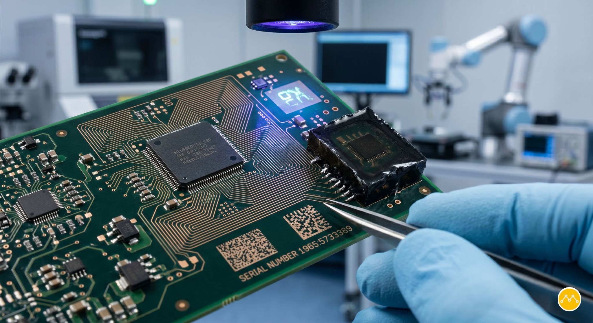
Why Solder Quality Affects Your High-Frequency PCB Performance: A Critical Analysis
Why Solder Quality Affects Your High-Frequency PCB Performance? High-frequency printed circuit boards operating at gigahertz frequencies demand exceptional signal integrity where even microscopic imperfections cause measurable performance degradation. While designers focus intensely on substrate materials, controlled impedance traces, and component selection, solder joint quality often receives insufficient attention despite its profound impact on signal transmission at elevated frequencies. Understanding how solder quality affects high-frequency PCB performance reveals why manufacturing process control separates reliable RF products from problematic designs plagued by intermittent failures and degraded specifications.
This comprehensive analysis examines the physical mechanisms through which solder quality impacts signal integrity, identifies critical defects affecting RF performance, and provides guidance on selecting manufacturing partners capable of delivering the precision high-frequency applications demand.

The Physics of High-Frequency Signal Transmission
At frequencies above 1 GHz, electrical signals behave as electromagnetic waves rather than simple voltages, fundamentally changing how circuit elements affect performance. Transmission line theory governs signal propagation, with characteristic impedance determined by trace geometry and dielectric properties. Any discontinuity in this carefully controlled impedance path—including solder joints—creates reflections that degrade signal quality.
The skin effect concentrates current flow near conductor surfaces at high frequencies, making surface quality and continuity critical. At 10 GHz, skin depth in copper measures approximately 0.66 micrometers, meaning signal current flows through an extremely thin surface layer. Surface roughness, voids, or contamination within this critical zone dramatically increases resistance and signal loss.
Solder joints connecting components to transmission lines represent potential impedance discontinuities if geometry deviates from design intent. A properly formed solder joint maintains impedance within ±5% tolerance, essential for minimizing return loss and preventing signal reflections. Poor solder joints create capacitive or inductive discontinuities that cause frequency-dependent signal degradation particularly problematic in broadband applications.
Critical Solder Defects Impacting RF Performance
Several solder defect types disproportionately affect high-frequency signal integrity compared to their impact on DC or low-frequency circuits.
Voids in solder joints represent one of the most insidious defects for high-frequency applications. These gas-filled cavities within solder create impedance mismatches and increase electrical resistance. Research indicates even 10% void content can degrade RF performance by 15-25% at frequencies above 5 GHz. Voids under ball grid array (BGA) components or thermal pads create particularly severe problems as they interrupt critical ground connections essential for controlled impedance.
X-ray inspection reveals void distribution, with industry standards targeting less than 5% void content for high-reliability RF applications. At millimeter-wave frequencies (24-52 GHz), virtually void-free solder joints become mandatory maintaining insertion loss specifications below 1dB per inch. Poor reflow profiles—particularly insufficient dwell time at peak temperature or excessive ramp rates—cause void formation through trapped flux volatiles or inadequate wetting.
Cold solder joints occur when insufficient heat prevents proper intermetallic compound formation between solder and pad metallization. These defective joints exhibit grainy, dull appearances rather than the smooth, shiny finish characteristic of quality solder. At RF frequencies, cold joints create frequency-dependent resistance through poor electrical contact. The high-resistance interface acts as a lossy transmission element causing signal attenuation and potentially generating harmonic distortion.
Temperature profiling during reflow critically affects solder joint quality. Profiles must achieve sufficient peak temperature (typically 240-260°C for lead-free solder) with adequate dwell time (60-90 seconds above liquidus) ensuring complete melting and intermetallic formation. Insufficient thermal mass in reflow ovens or improper conveyor speed creates temperature variations across boards causing cold joints in cooler regions while potentially damaging components in hotter areas.
Solder bridges connecting adjacent pads or traces create parasitic capacitance shifting resonant frequencies and degrading impedance matching. At high frequencies, even small capacitive loads significantly impact circuit behavior. A bridge adding 0.5pF capacitance causes noticeable performance changes in 5 GHz circuits. Beyond electrical effects, solder bridges can create intermittent shorts causing mysterious failures difficult to diagnose.
Insufficient solder leaves gaps or incompletely filled fillets reducing contact area and increasing resistance. While DC continuity may test acceptable, the reduced cross-section increases high-frequency resistance through skin effect limitations. Insufficient solder often results from inadequate solder paste deposition, improper stencil design, or insufficient flux activation during reflow.
Excessive solder creates uncontrolled geometry affecting characteristic impedance particularly for surface mount components on transmission lines. While ensuring electrical connection, excess solder forms bulbous joints with unpredictable electromagnetic properties. For controlled impedance applications, solder joint dimensions must fall within design tolerances maintaining impedance specifications.
Impedance Discontinuities and Signal Integrity
High-frequency circuits require controlled characteristic impedance—typically 50 ohms for RF applications or 75 ohms for video/antenna connections—maintained along the entire signal path. Solder joints connecting components to transmission lines create transition regions where impedance variations must be minimized.
Proper solder joint geometry approximates the designed transmission line structure maintaining impedance continuity. Poor soldering creates abrupt impedance changes causing partial signal reflection back toward the source. The magnitude of reflection depends on the impedance mismatch severity, quantified by return loss measurements. Return loss below -10dB indicates acceptable matching, while values below -15dB represent excellent performance. Poor solder joints can degrade return loss to -5dB or worse, reflecting 30% of signal power.
Time-domain reflectometry (TDR) measurements reveal impedance variations along signal paths including solder joint regions. Quality solder joints appear as minimal impedance perturbations on TDR traces, while defective joints show clear impedance spikes correlating with physical discontinuities. Vector network analyzers (VNA) characterize frequency-domain performance through S-parameter measurements revealing insertion loss and return loss across the operating frequency range.
Manufacturing process control maintaining consistent solder joint geometry ensures impedance stability across production quantities. Variation in solder volume, wetting behavior, or pad metallization creates board-to-board performance differences unacceptable for high-volume RF products requiring tight specifications.
Surface Finish and Intermetallic Formation
PCB surface finish selection critically affects solder joint quality and high-frequency performance. Electroless nickel immersion gold (ENIG) provides popular finish for RF boards offering flat surfaces, excellent solderability, and corrosion resistance. However, the nickel layer’s ferromagnetic properties introduce frequency-dependent losses particularly above 5 GHz. Studies indicate ENIG can contribute 0.1-0.2dB per inch insertion loss at 10 GHz depending on trace geometry.
The gold layer in ENIG (typically 2-5 microinches) provides low-resistance surface minimizing skin effect losses. Proper ENIG processing ensures gold thickness remains within specifications—excessive gold creates brittle intermetallic compounds during soldering potentially causing reliability issues, while insufficient gold allows nickel oxidation degrading solderability.
Immersion silver offers lower insertion loss than ENIG due to absence of nickel layer, making it attractive for frequencies above 10 GHz. However, silver tarnishes more readily requiring careful handling and storage. Organic solderability preservative (OSP) provides minimal signal loss but offers limited shelf life and single reflow capability restricting its use to controlled manufacturing environments.
Intermetallic compound formation at the solder-pad interface provides mechanical strength and electrical continuity. Proper reflow profiles create thin, uniform intermetallic layers (1-3 micrometers) providing reliable connections. Insufficient reflow temperatures or times prevent adequate intermetallic formation creating weak, high-resistance joints. Excessive intermetallic growth from prolonged thermal exposure or multiple reflows creates brittle joints prone to cracking under thermal cycling or mechanical stress.
Manufacturing Process Controls for High-Frequency Assembly
Achieving consistent solder quality for high-frequency PCBs requires sophisticated manufacturing processes exceeding typical electronics assembly standards.
Reflow profiling represents the foundation of quality solder joints. Proper profiles balance multiple requirements: gradual preheat (1-3°C per second ramp rate) activates flux and brings boards to temperature uniformly, soak zone (150-180°C for 60-120 seconds) allows thermal equalization preventing component damage, peak temperature (240-260°C for lead-free) ensures complete melting and intermetallic formation, and controlled cooling prevents thermal shock. Temperature variations across the board must remain within ±2°C maintaining process consistency.
Modern reflow ovens use multiple heating zones with independent control enabling precise profiling. Forced convection heating improves temperature uniformity compared to IR heating alone. For high-frequency boards using specialized materials like Rogers substrates, reflow profiles must account for different thermal properties compared to standard FR4.
Solder paste selection affects joint quality through particle size distribution, flux chemistry, and metal content. For fine-pitch components common in RF designs, Type 4 or Type 5 solder paste with smaller particles improves print definition preventing bridging. Flux chemistry must provide adequate wetting without leaving corrosive residues interfering with signal integrity. No-clean flux formulations minimize residue but require careful process validation ensuring acceptable soldering results.
Stencil design controls solder paste deposition with precision critical for high-frequency applications. Aperture size, shape, and wall finish affect paste release and deposition accuracy. For BGAs and QFNs, aperture dimensions typically range from 80-120% of pad size depending on component pitch and solder joint requirements. Electropolished stencils or laser-cut stencils provide smoother aperture walls improving paste release compared to chemically etched stencils.
Automated optical inspection (AOI) identifies solder defects through high-resolution imaging and sophisticated algorithms. Modern AOI systems detect insufficient solder, solder bridges, component misalignment, missing components, and surface defects. For high-frequency assemblies, AOI validation becomes essential catching defects before boards reach testing stages where diagnosis becomes more difficult and expensive.
X-ray inspection reveals hidden defects in BGAs, QFNs, and other bottom-terminated components where traditional optical inspection cannot assess solder joint quality. X-ray systems measure void percentage, verify solder coverage, and detect inadequate fillet formation. For RF applications, targeting less than 5% void content ensures reliable signal transmission. Three-dimensional X-ray tomography provides complete volumetric analysis of solder joints enabling detailed failure analysis when problems occur.
Testing and Validation for High-Frequency Performance
Quality solder joints must be verified through electrical testing confirming signal integrity meets specifications.
In-circuit testing (ICT) validates electrical connectivity detecting opens, shorts, and component value verification. While essential for catching gross defects, ICT typically operates at low frequencies inadequate for validating high-frequency performance. Flying probe testers provide flexible testing without dedicated fixtures beneficial for prototype quantities.
Vector network analysis characterizes high-frequency performance through S-parameter measurements. S11 (return loss) quantifies impedance matching, while S21 (insertion loss) measures signal transmission efficiency. Quality RF assemblies maintain S11 below -10dB across the operating frequency range with insertion loss minimized according to application requirements. Measuring S-parameters on production boards validates solder joint quality and identifies boards with performance degradation indicating assembly defects.
Time-domain reflectometry identifies impedance discontinuities along signal paths including solder joint regions. TDR measurements reveal the location and magnitude of impedance variations enabling correlation between physical defects and electrical performance. Comparing TDR signatures across multiple boards quantifies manufacturing consistency essential for high-volume production.
Functional testing validates complete circuit operation under realistic conditions. For RF products, this includes transmit power measurements, receiver sensitivity testing, frequency accuracy verification, and modulation quality assessment. Functional testing catches problems that electrical parameter testing might miss confirming assembled boards meet all performance specifications.
Choosing Manufacturing Partners for High-Frequency Success
The complexity of high-frequency PCB assembly demands manufacturing partners with specialized capabilities and proven experience in RF applications.
Process capability and equipment separate professional RF assembly from general electronics manufacturing. Look for manufacturers operating modern reflow ovens with precise profiling capabilities (±2°C control across zones), comprehensive inspection equipment including AOI and X-ray systems, vector network analyzers for S-parameter characterization, and environmental controls maintaining temperature and humidity within specifications preventing moisture-related defects.
Quality certifications provide objective evidence of manufacturing capability. ISO 9001:2015 certification demonstrates quality management systems commitment. IPC-A-610 Class 3 compliance ensures workmanship meets high-reliability standards essential for RF applications. AS9100 certification for aerospace applications or ISO 13485 for medical devices indicates experience with demanding quality requirements.
Material and substrate experience matters particularly for high-frequency designs using specialized materials. Rogers, PTFE, and other high-frequency laminates require different handling and processing compared to standard FR4. Manufacturers experienced with these materials understand proper reflow profiles, drilling parameters, and assembly techniques preventing damage or performance degradation.
Design for manufacturability support helps optimize designs for reliable assembly. Experienced RF manufacturers provide DFM feedback identifying potential assembly challenges including pad geometries requiring adjustment, component placements creating shadowing during reflow, and test point access for validation. This collaborative approach catches issues before fabrication preventing expensive redesigns.
Testing and validation capabilities distinguish manufacturers capable of validating high-frequency performance from those offering only basic electrical testing. Request evidence of S-parameter testing capability, impedance measurement procedures, and quality control protocols specific to RF assemblies. Manufacturers maintaining test data and providing documented results demonstrate commitment to quality beyond simple pass/fail assessments.
Companies like MorePCB exemplify comprehensive high-frequency PCB capabilities combining advanced fabrication with precision assembly services. Their expertise spans high-frequency substrate materials including Rogers and PTFE for optimal signal integrity, controlled impedance manufacturing maintaining ±5% tolerance through proven processes, multilayer and HDI technology enabling complex RF designs, comprehensive assembly services with AOI and X-ray inspection, and global shipping delivering RF products worldwide supporting international development teams.
Quality certifications including ISO 9001:2015 and IPC standards compliance ensure consistent manufacturing meeting industry requirements. Engineering support assists with material selection, impedance calculations, and DFM optimization improving designs before production begins. This partnership approach treats high-frequency PCB manufacturing as collaborative process rather than simple order fulfillment.
Preventing Solder Quality Issues Through Design
While manufacturing process control ensures quality execution, design decisions significantly impact solder joint reliability and high-frequency performance.
Pad geometry optimization provides adequate area for solder fillet formation while minimizing parasitic effects. For RF applications, pad dimensions should accommodate component terminations with minimal excess area. Excessive pad size increases capacitance affecting impedance, while insufficient pad area creates weak solder joints prone to failure.
Thermal relief design balances electrical connection with thermal management. Solid connections to ground planes create excessive thermal mass preventing proper solder reflow. Thermal relief patterns (typically four 0.3-0.5mm spokes) maintain electrical continuity while allowing controlled heat flow during soldering. For high-frequency grounds, thermal reliefs must maintain low inductance avoiding signal integrity degradation.
Via design affects both manufacturability and electrical performance. Thermal vias beneath power components require careful consideration balancing thermal dissipation with solder joint quality. Excessive via density can create solder wicking into vias rather than forming proper surface fillets. Filled or plugged vias prevent solder wicking while maintaining flat component mounting surfaces.
Component selection considering assembly compatibility prevents problems during manufacturing. Fine-pitch BGAs with 0.4mm pitch or smaller require precise placement and reflow control beyond basic assembly capabilities. QFN packages with exposed thermal pads demand adequate solder paste deposition and proper reflow profiling avoiding voids. Selecting components within manufacturer capabilities ensures reliable assembly.
The intersection of solder quality and high-frequency performance represents a critical yet often underappreciated aspect of RF product development. Understanding the physical mechanisms through which solder defects degrade signal integrity empowers designers to make informed decisions about manufacturing partners and assembly processes. As operating frequencies continue increasing in modern electronics—from 5G communication to automotive radar to satellite systems—the demands on solder quality intensify proportionally. Success requires combining thoughtful design practices with professional manufacturing expertise ensuring every solder joint meets the exacting standards high-frequency applications demand. Whether developing prototype RF modules or scaling to production volumes, partnering with experienced manufacturers who understand and control the critical variables affecting solder quality makes the difference between reliable products and those plagued by mysterious performance issues traceable to inadequate assembly processes.
Frequently Asked Questions
How does solder quality affect high-frequency PCB signal integrity?
Solder quality directly impacts high-frequency PCB signal integrity through multiple interconnected mechanisms. Poor solder joints create impedance discontinuities causing signal reflections, with each discontinuity potentially adding 0.5-2dB insertion loss at 10GHz frequencies. Voids in solder joints increase electrical resistance by 15-40% causing signal attenuation and localized heating that can damage components. Cold solder joints with grainy, high-resistance interfaces create frequency-dependent losses particularly problematic above 5GHz where skin effect concentrates current in surface layers. Surface roughness from improper soldering increases skin effect losses at high frequencies. Quality solder joints with smooth interfaces, minimal voids (target <5% for RF applications), and proper intermetallic compound formation maintain controlled impedance within the ±5% tolerance required for signal integrity above 1GHz, ensuring return loss below -10dB and insertion loss meeting design specifications across the operating frequency range.
What solder defects most impact RF circuit performance?
Critical solder defects affecting RF circuit performance include voids in solder joints particularly under BGAs and thermal pads creating impedance mismatches and increased insertion loss of 0.2-0.8dB per significant void, cold solder joints with insufficient intermetallic formation causing frequency-dependent resistance that degrades signal amplitude and introduces distortion, solder balls or bridges between adjacent traces creating parasitic capacitance of 0.2-1.0pF shifting resonant frequencies and degrading impedance matching, insufficient solder creating high-resistance connections with increased skin effect losses above 1GHz, and excessive solder creating uncontrolled geometry affecting characteristic impedance through parasitic capacitance and inductance. At frequencies above 5GHz, even 10% void content can degrade overall performance by 15-25% through combined effects of resistance increase and impedance mismatch. For millimeter-wave applications operating at 24-52GHz, virtually void-free solder joints (under 2% void content) are essential maintaining insertion loss specifications below 1dB per inch required for reliable signal transmission.
Why is impedance control critical in high-frequency solder joints?
Impedance control in solder joints is critical because high-frequency signals behave as electromagnetic waves requiring constant characteristic impedance (typically 50Ω for RF applications or 75Ω for antenna connections) along the entire signal path from source to load. Solder joints connecting components to transmission lines create potential impedance discontinuities if geometry deviates from design specifications. Properly formed solder joints with controlled dimensions maintain impedance within ±5% tolerance preventing signal reflections that cause return loss degradation. Poor solder geometry creates capacitive or inductive discontinuities introducing frequency-dependent effects. At 10GHz, a 10% impedance variation can cause return loss of -14dB or worse, reflecting 25% of signal power back toward the source creating standing waves and degrading performance. Quality manufacturers use precise reflow profiling maintaining ±2°C temperature control across boards ensuring consistent solder joint geometry. Controlled impedance verification through time-domain reflectometry or vector network analysis confirms solder joints maintain specified impedance across the frequency spectrum, with S11 measurements below -15dB indicating excellent impedance matching essential for reliable high-frequency operation.
How do manufacturing processes ensure high-frequency solder quality?
Professional manufacturers ensure high-frequency solder quality through comprehensive process controls including precise reflow profiling with multi-zone ovens maintaining ±2°C temperature control preventing cold joints and thermal damage, automated optical inspection (AOI) with high-resolution cameras detecting placement errors and surface solder defects, X-ray inspection revealing hidden voids in BGAs and QFNs targeting less than 5% void content for RF applications, controlled atmosphere reflow using nitrogen to reduce oxidation and improve wetting, optimized solder paste with Type 4 or Type 5 particle size distribution for fine-pitch components, IPC-A-610 Class 3 workmanship standards ensuring high-reliability connections suitable for aerospace and medical applications, vector network analyzer testing measuring S-parameters confirming signal integrity meets specifications, and comprehensive documentation including temperature profiles, inspection results, and electrical test data. Quality manufacturers implement statistical process control tracking void rates, solder joint consistency, defect rates, and electrical performance metrics ensuring every board meets specifications for high-frequency operation with documented traceability supporting quality investigation if issues arise.
When should I choose professional assembly for high-frequency PCBs?
Professional assembly becomes essential for high-frequency PCBs operating above 1GHz requiring controlled impedance within ±5% tolerance impossible to achieve with hand assembly methods, RF circuits containing BGAs, QFNs, or fine-pitch components (0.5mm pitch or smaller) demanding precision pick-and-place equipment and void-free solder joints, applications requiring documented testing including S-parameter verification, time-domain reflectometry, and impedance measurement demonstrating compliance with specifications, production quantities where consistency across boards is critical maintaining ±2dB performance variation across batches, designs using specialized materials like Rogers or PTFE substrates requiring compatible reflow profiles and handling procedures, and products requiring regulatory certification (FCC, CE) demanding documented manufacturing processes and quality systems. Manufacturers like MorePCB offer comprehensive high-frequency PCB capabilities including Rogers and PTFE substrate fabrication expertise, controlled reflow processes with validated temperature profiling, AOI and X-ray inspection targeting less than 5% void content, impedance testing and S-parameter verification using vector network analyzers, IPC-A-610 Class 3 workmanship standards, and global shipping supporting RF product development worldwide. For frequencies above 10GHz or critical applications including 5G infrastructure, automotive radar systems, satellite communication, or aerospace electronics, professional assembly with proven high-frequency capabilities ensures reliable signal integrity and product success.